►Know-how
The Nano-Rennes platform is equipped with a set of equipment dedicated to the growth of III-V and / or silicon materials.
It has a strong experience in the growth of materials on InP substrates, as well as the low temperature growth (<200 ° C) of Si-based compounds.
It benefits from a know-how in growth of :
- Materials of the InP technology : InP, InAs, InGaAs, InAlAs, InAsP, In1-xGaxAsyP1-y (1,18µm <l<1,6µm) sur InP(100) et InP(311)B, InGaAlAs, GaAsSb, AlAsSb. BQ InAs sur InP(311)B, Qdash InAs sur InP(100) (1,5µm<l<1,8µm)
- Materials of the GaAs technology : GaAs, AlAs, InGaAs, AlGaAs
- Materials of the GaPtechnology : GaP, AlP, GaAsP, GaAlP
- Materials of the Si technology : Si
►Description of growth equipment
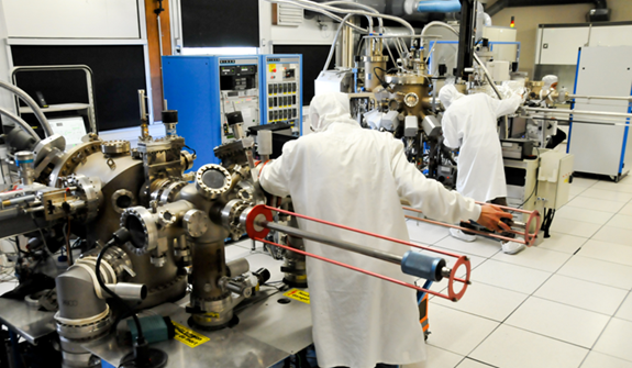
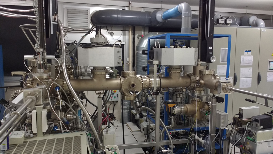
GS-MBE (gas state molecular beam epitaxy) : RIBER32 (FOTON-INSA)
- Elements III (solids) : In1, In2, Ga1, Ga2, Si, Be
- Elements V (gas) : PH3, AsH3,
Dping Si, Be, C (CBr4 gas cell)
Specificities :
- Wafers 2 inches
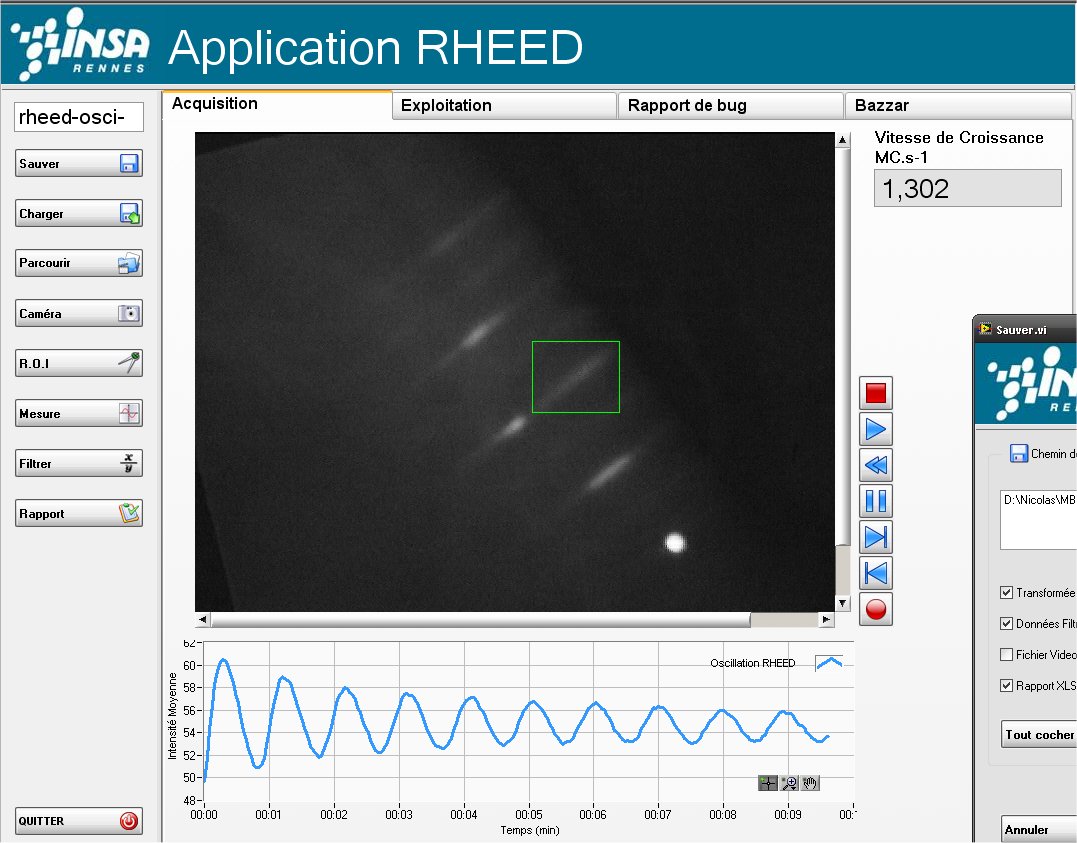
- Ultra-void (10-10 mbar)
- RHEED
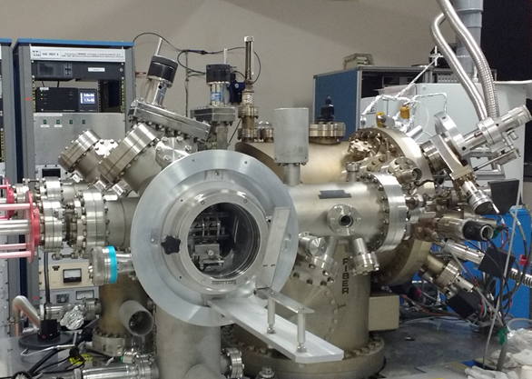
SS-MBE (solid state molecular beam epitaxy) : RIBER (FOTON-INSA) COMPACT21
- Elements III (solids) : In1, In2, Ga1, Ga2, Al doping (Si, Be)
- Elements V (cracker) : P4, As4, Sb4, N2 (plasma cell)
Specificities :
- Wafers 2 inches
- Ultra-void (10-10 mbar)
- RHEED (20keV)
- In-sity transfert to the UHV-LPCVD frame
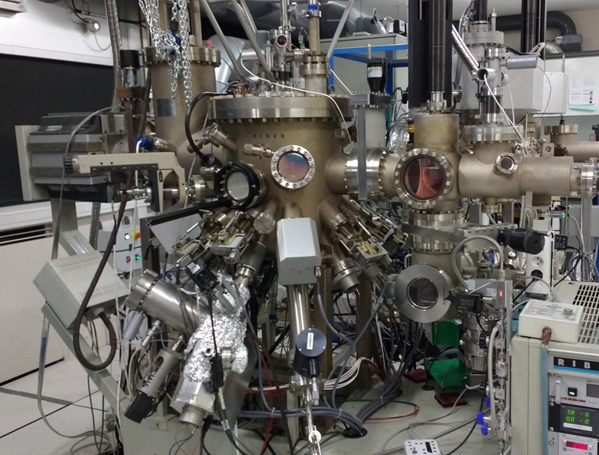
UHV-LPCVD (ultra high vaccum-low pressure chemical vapor deposition) : RIBER (FOTON-INSA)
- Elements : SiH4, AsH3, B2H6
Specificities :
- Rheed (30keV)
- Wafers 2 inches
- Ultra-void (10-10 mbar)
- In-situ UHV transfert to the SSMBE frame
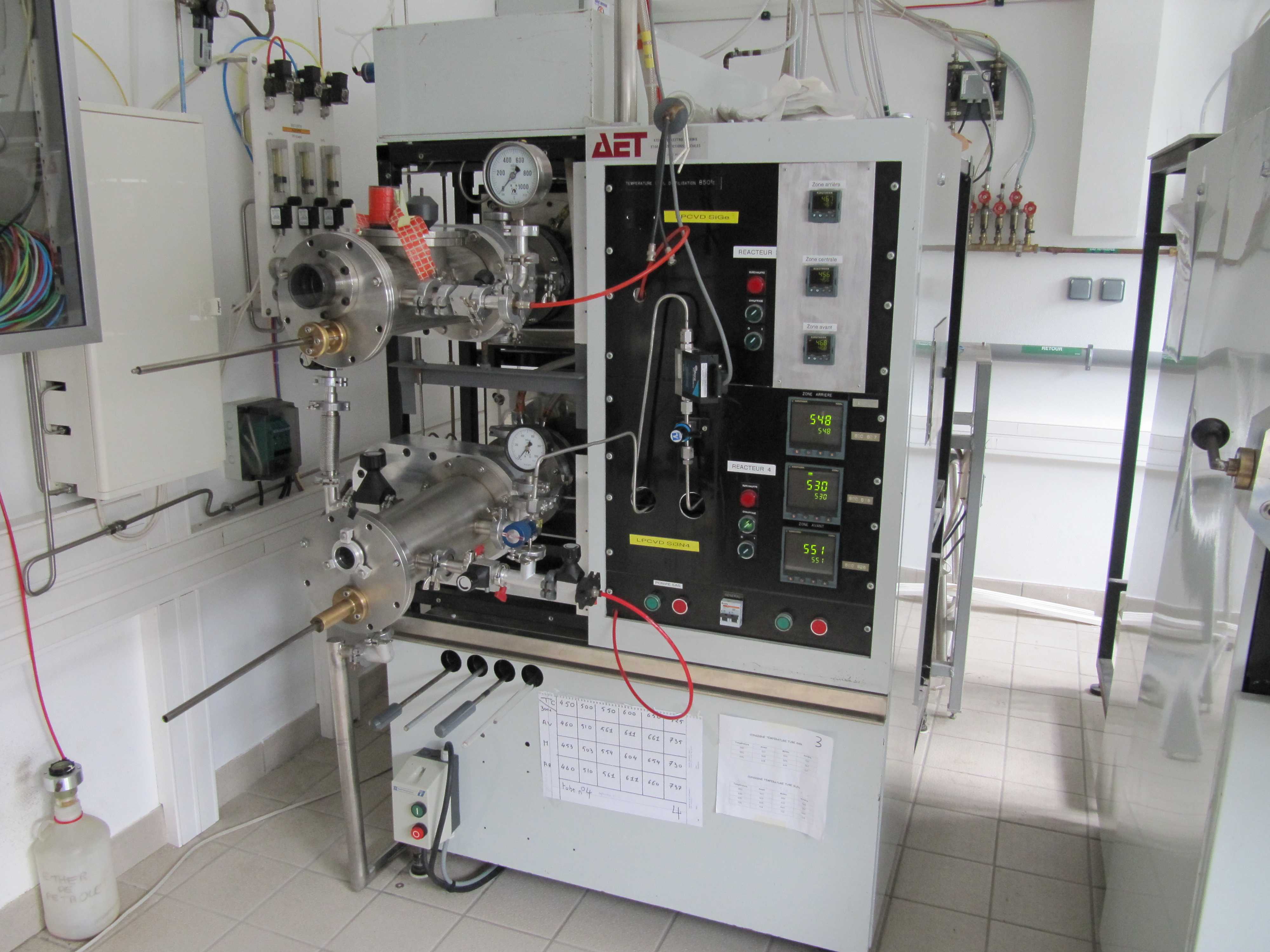
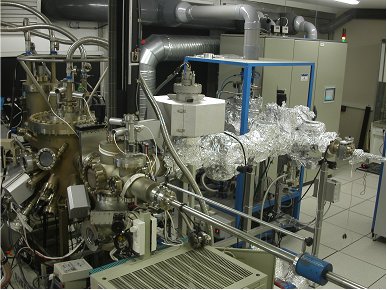
4 LPCVD (low pressure chemical vapor deposition) : AET (IETR-GM)
- Elements : SiH4, GeH4, PH3, AsH3, B2H6, He, N2
Specificities :
- Wafers 2 inches max
- Low and high temperature growth
- Secondary void (10-6 mbar)
APCVD (atmospheric pressure chemical vapor deposition) : TEMPRESS (IETR-GM)
- Elements : SiH4, O2, N2
Specificities :
- Wafers 2 inches max
- Low temperature growth of SiO2 (<200 °C)
- Primary void (10-3 mbar)
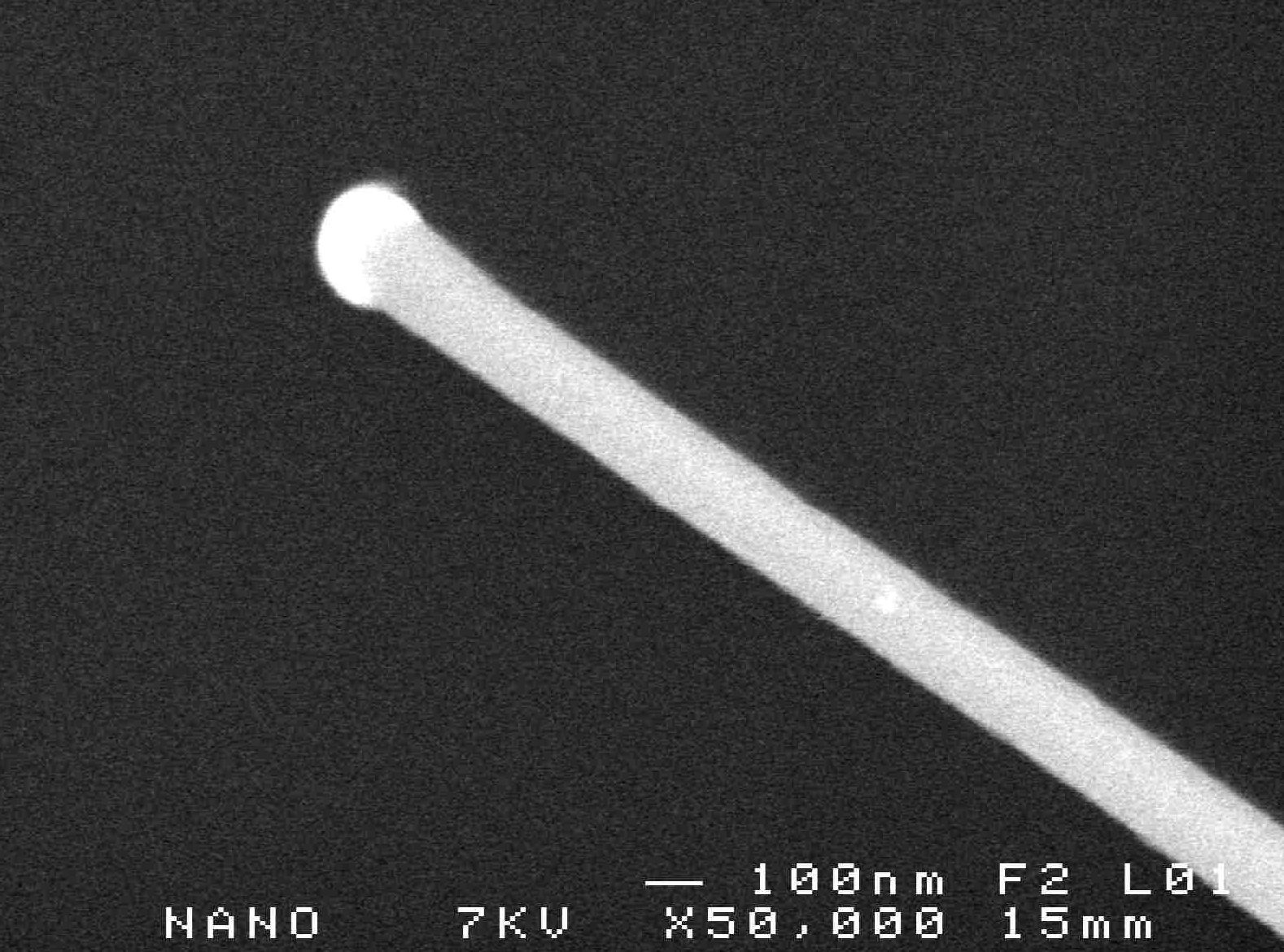
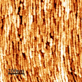
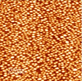
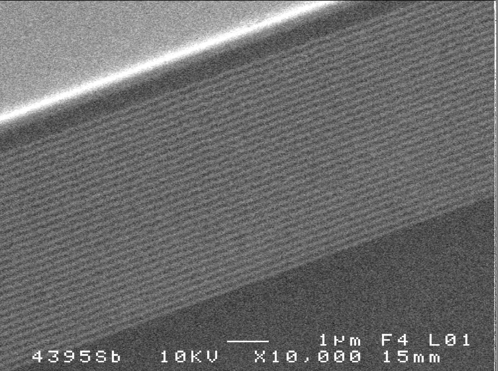
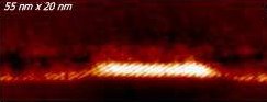
►Examples of achievements