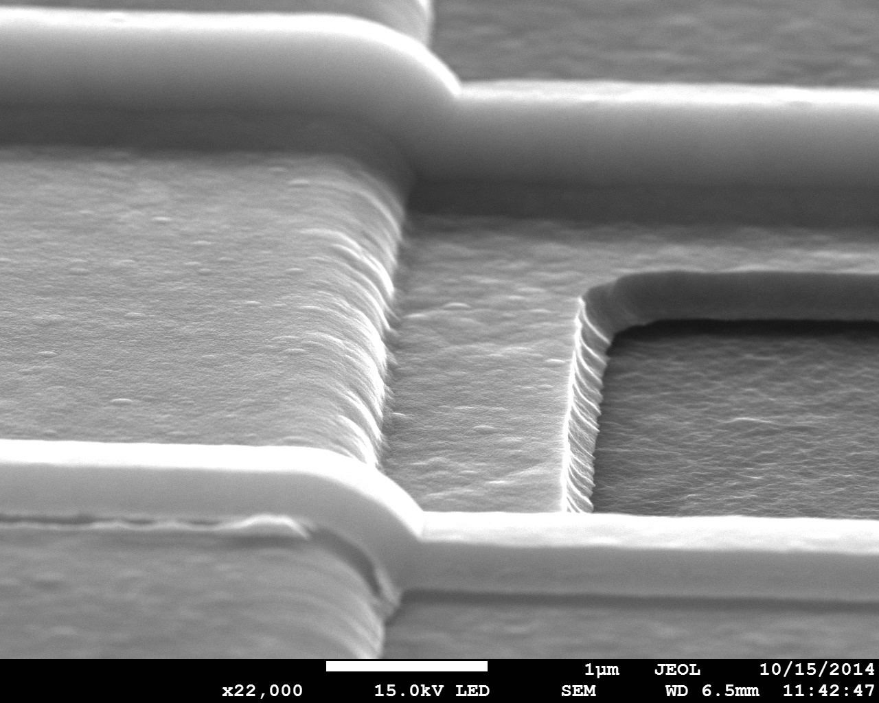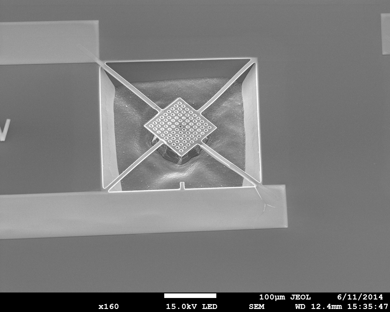
Nanorennes areas of expertises cover mainly nano-micrometer sized technologies for the fabrication of devices in microelectronic, optoelectronic, as well as chemical and bio physics. The main originality of the platform is to gather on the same site important know-how in the growth and processing of silicon and III-V compound (mainly InP and GaP).
Nanorennes benefits of a great experience in :
- sensors fabrications (MEMs, bio-chemical sensors)
- quantum nanostructures gowth (quantum wels, wires, dots)
- low temperature growth and processing of silicon based devices (TFTs, sensors on flexible subtrates)
- photonic technologies (edge emitting lasers, VCSELs, solar cells)
- heterogeneous and homogeneous integration of optoelectronic and microelectronic (III-V growth on Si, bonding on Si)