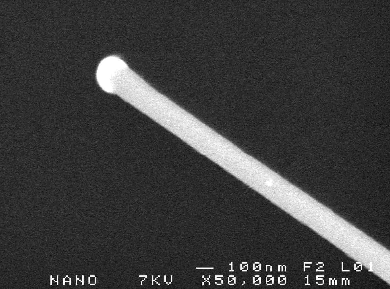
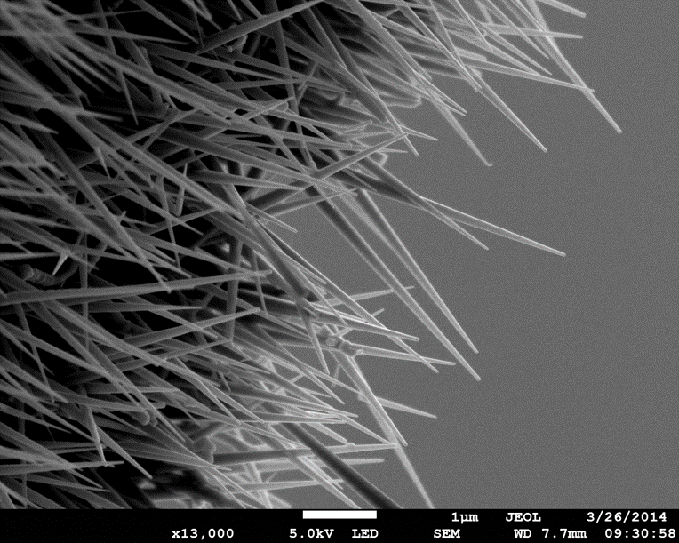
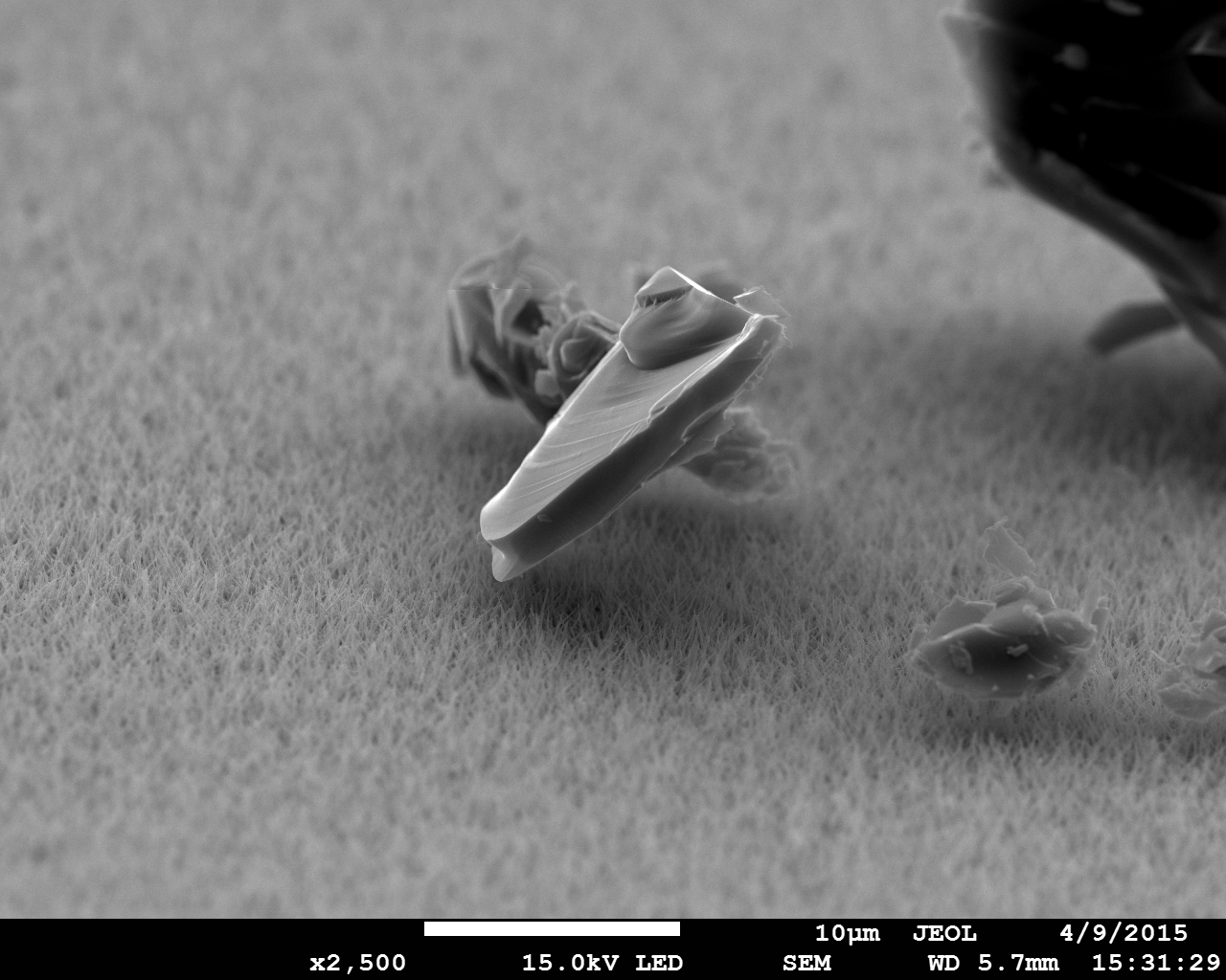
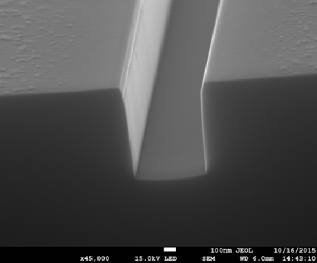
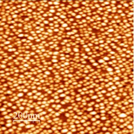
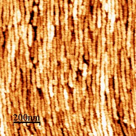
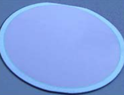
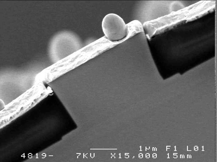
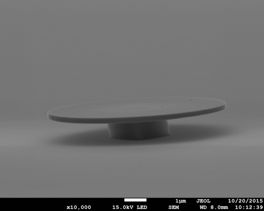
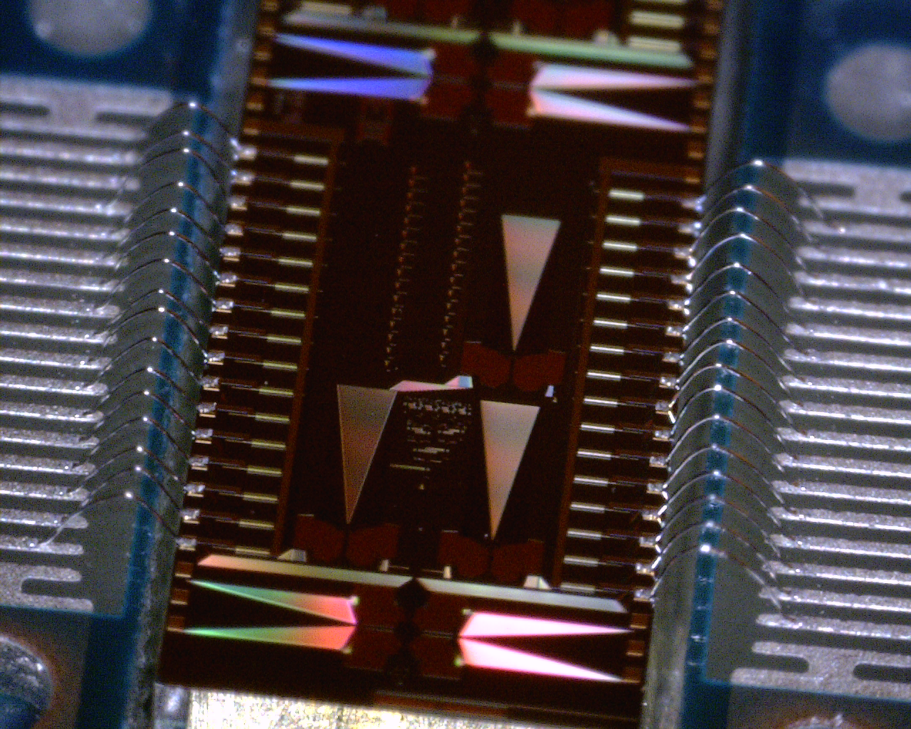
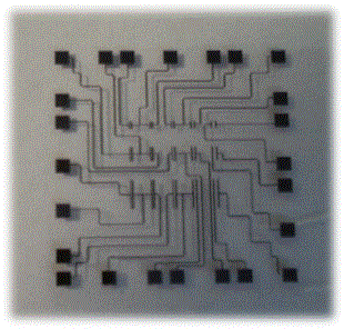
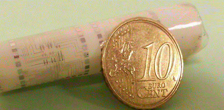
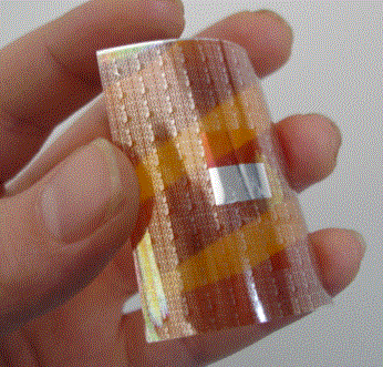
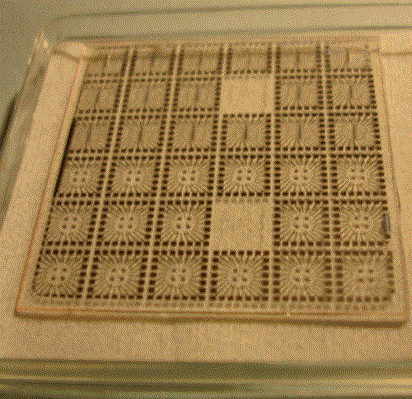
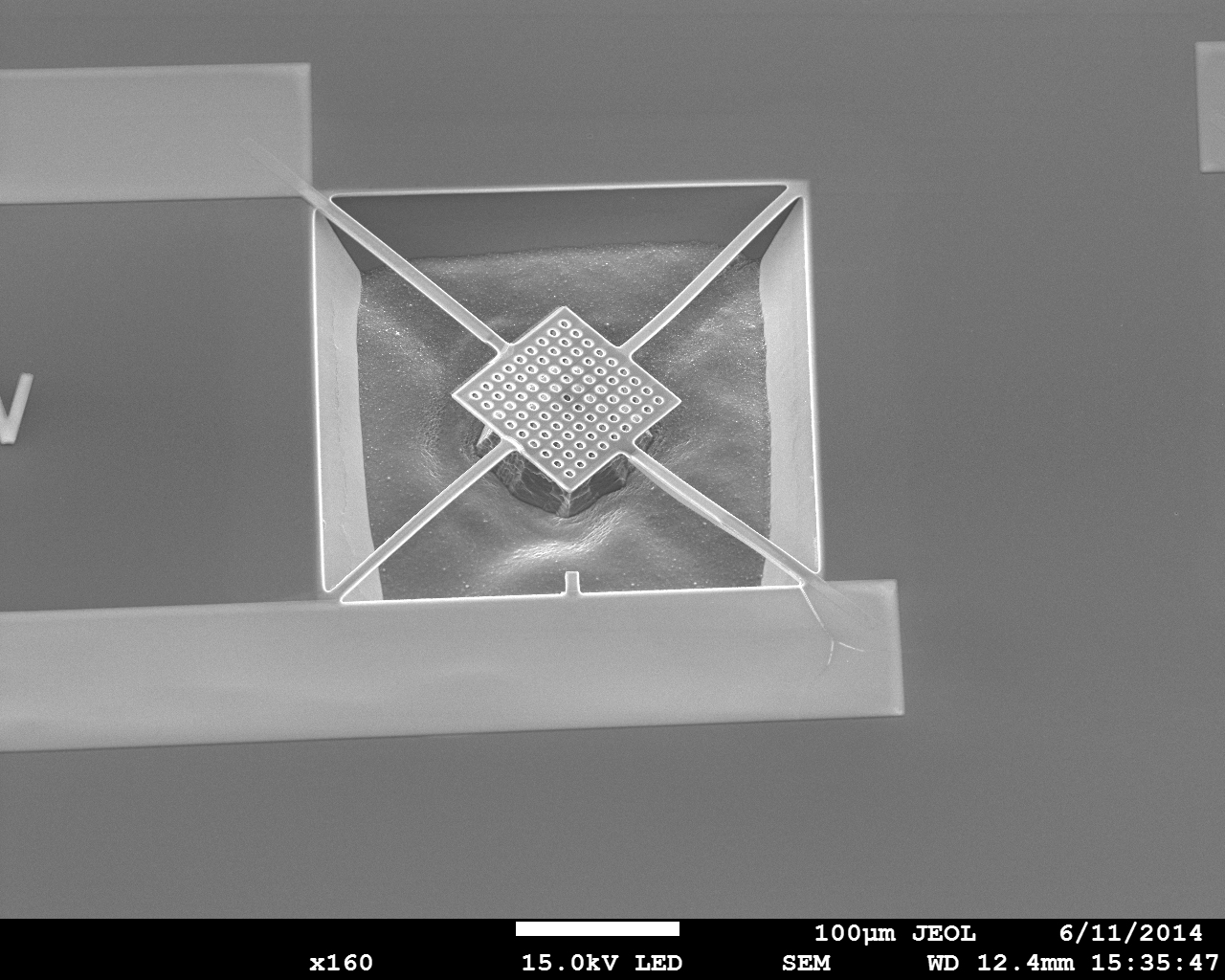
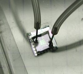
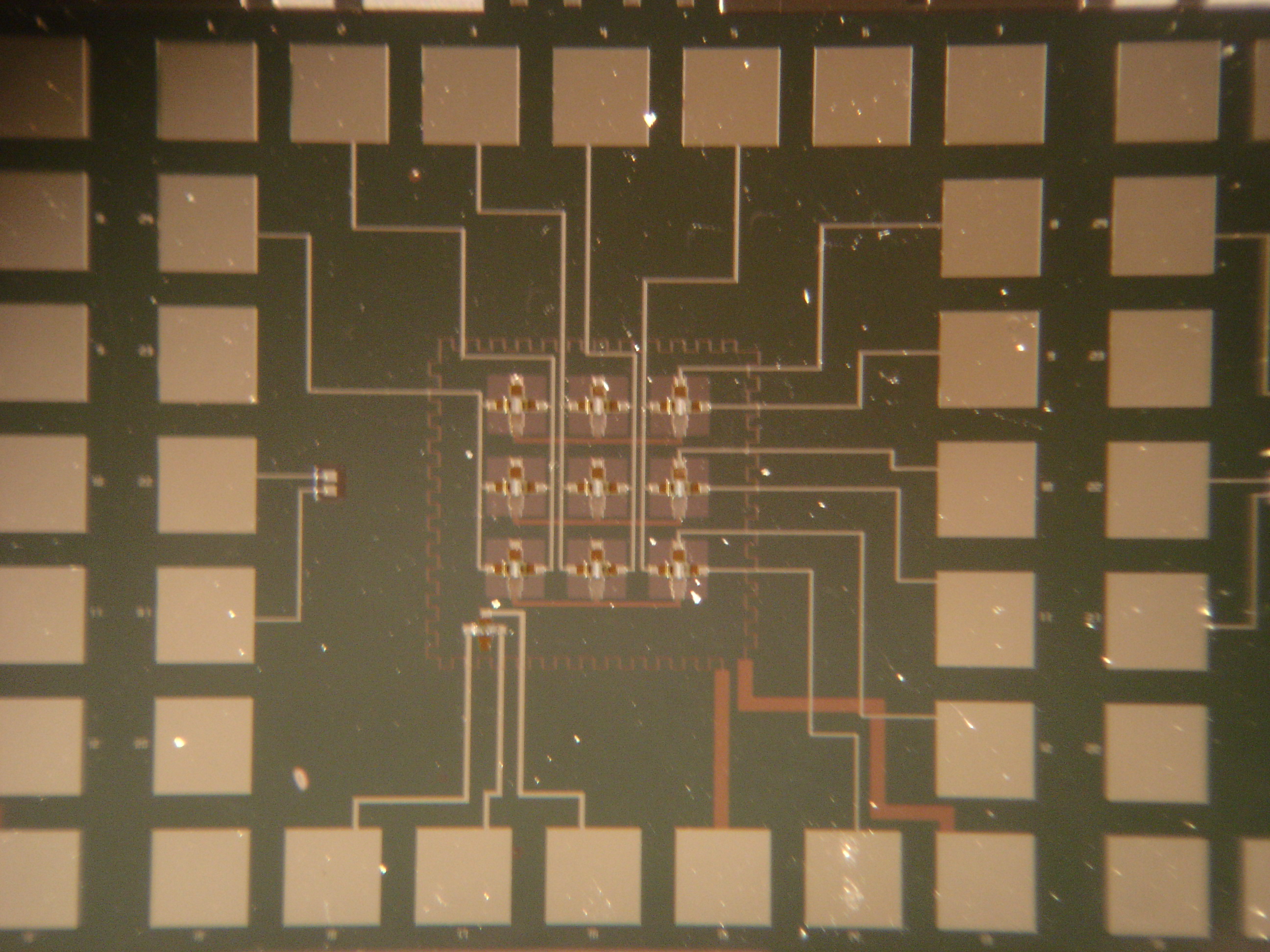
►Materials and nanostructures Si nano wires by VLS growth Ge nano wires by VLS growth Super hydrophobic surface (lotus) Trench type engraving of Si High density of InAs QDs on InP (113) B 2 * 2 μm² AFM image High density of quantum dots on InP (001) 2 * 2 μm² AFM image Growth of GaP on Si substrate 2 inches ►Photonic components Laser GaP micro-disk VCSEL on InP Optical amplifier Micro wiring of photonic chips ►Microelectronic components Printed electronic Organic electronic on paper µ-Si electronic on Kapton Poly-Si electronic on glass ►Biochemical components & MEMS Bolometer on suspended membrane Suspended cantilever in nitride of Si Sensor coupled with micro-fluidic circuit Sensor array on Si-mono